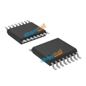

CD40109BPWRE4
- Manufacturer’s Part#:CD40109BPWRE4
- Manufacturer:
- Categories:
- Sub-Categories:
- Series:4000B
- ECAD Model:
- Description:IC TRNSLTR UNIDIR 16TSSOP
- Quantity:RFQAdd to RFQ List
- Payment:

- Delivery:

- In Stock: 628503
- Available: 4000
Reference Price(In US Dollars)
| Qty | Unit Price | Ext.Price |
|---|---|---|
| 1+ | US $0.43245 | US $0.43 |
| 10+ | US $0.28830 | US $2.88 |
| 30+ | US $0.21623 | US $6.49 |
| 100+ | US $0.17298 | US $17.30 |
| 500+ | US $0.15857 | US $79.29 |
| 1000+ | US $0.14415 | US $144.15 |
Do you want a lower wholesale price? Please send us an inquiry, and we will respond immediately.
- Description
- Alternatives
- Shopping Guide
The CD40109BMS, unlike other low-to-high level shifting circuits, does not require the presence of the high voltage supply (VDD) before the application of either the low voltage supply (VCC) or the input signals.
There are no restrictions on the sequence of application of VDD, VCC, or the input signals. In addition, with one exception there are no restrictions on the relative magnitudes of the supply voltages or input signals within the device maximum ratings, provided that the input signal swings between VSS and at least 0.7VCC; VCC may exceed VDD, and input signals may exceed VCC and VDD. When operated in the mode VCC > VDD, the CD40109BMS will operate as a high-to-low level shifter.
Features
• High Voltage Type (20V Rating)
• Independence of Power Supply Sequence Considerations - VCC can Exceed VDD - Input Signals can Exceed Both VCC and VDD
• Up and Down Level Shifting Capability
• Three-State Outputs with Separate Enable Controls
• 100% Tested for Quiescent Current at 20V
• 5V, 10V and 15V Parametric Ratings
• Maximum Input Current of 1µA at 18V Over Full Package Temperature Range; 100nA at 18V and +25oC
• Noise Margin (Over Full Package/Temperature Range) - 1V at VCC = 5V, VDD = 10V - 2V at VCC = 10V, VDD = 15V
• Standardized Symmetrical Output Characteristics
• Meets All Requirements of JEDEC Tentative Standard No. 13B, “Standard Specifications for Description of ‘B’ Series CMOS Devices”Applications
• High or Low Level Shifting with Three-State Outputs for Unidirectional or Bidirectional Bussing
• Isolation of Logic Subsystems Using Separate Power Supplies from Supply Sequencing, Supply Loss and Supply Regulation Considerations
Functional Equivalent (FE) materials, including Fused Filament Fabrication (FFF) form, assembly, and functionally compatible substitute materials.
SHIPPING GUIDE
Shipping Methods

Rest assured that your orders will be handled by these trusted providers, such as DHL, FedEx, SF, and UPS.
Shipping Cost

Shipping starts at $40 but varies for destinations like South Africa, Brazil, India, and more. The actual shipping charges depend on time zone, country, and package weight/volume.
Delivery Time

We ship orders once daily, around 5 p.m., except on Sundays. The estimated delivery time may vary depending on the courier service you choose, but typically ranges from 5 to 7 business days.

Professional Platform

Full-speed Delivery

Wide Variety of Products

365 Days of Quality Assurance


