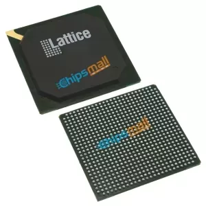

LFE3-150EA-8FN672C
- Manufacturer’s Part#:LFE3-150EA-8FN672C
- Manufacturer:
- Categories:
- Sub-Categories:
- Series:ECP3
- ECAD Model:
- Description:IC FPGA 380 I/O 672FBGA
- Datasheet:
- Quantity:RFQAdd to RFQ List
- Payment:

- Delivery:

- Available: 630
Reference Price(In US Dollars)
| Qty | Unit Price | Ext.Price |
|---|---|---|
| 1+ | US $93.20000 | US $93.20 |
| 10+ | US $69.90000 | US $699.00 |
| 30+ | US $60.58000 | US $1817.40 |
| 100+ | US $53.59000 | US $5359.00 |
| 500+ | US $50.32800 | US $25164.00 |
| 1000+ | US $46.60000 | US $46600.00 |
Do you want a lower wholesale price? Please send us an inquiry, and we will respond immediately.
- Description
- Alternatives
- Shopping Guide
The LatticeECP3™ (EConomy Plus Third generation) family of FPGA devices is optimized to deliver high performance features such as an enhanced DSP architecture, high speed SERDES and high speed source synchronous interfaces in an economical FPGA fabric. This combination is achieved through advances in device architecture and the use of 65 nm technology making the devices suitable for high-volume, high-speed, low-cost applications.
Features
• Higher Logic Density for Increased System Integration
• 17K to 149K LUTs
• 116 to 586 I/Os
• Embedded SERDES
• 150 Mbps to 3.2 Gbps for Generic 8b10b, 10-bit SERDES, and 8-bit SERDES modes
• Data Rates 230 Mbps to 3.2 Gbps per channel for all other protocols
• Up to 16 channels per device: PCI Express, SONET/SDH, Ethernet (1GbE, SGMII, XAUI), CPRI, SMPTE 3G and Serial RapidIO
• sysDSP™
• Fully cascadable slice architecture
• 12 to 160 slices for high performance multiply and accumulate
• Powerful 54-bit ALU operations
• Time Division Multiplexing MAC Sharing
• Rounding and truncation
• Each slice supports — Half 36x36, two 18x18 or four 9x9 multipliers — Advanced 18x36 MAC and 18x18 Multiply-Multiply-Accumulate (MMAC) operations
• Flexible Memory Resources
• Up to 6.85Mbits sysMEM™ Embedded Block RAM (EBR)
• 36K to 303K bits distributed RAM
• sysCLOCK Analog PLLs and DLLs
• Two DLLs and up to ten PLLs per device
• Pre-Engineered Source Synchronous I/O
• DDR registers in I/O cells
• Dedicated read/write levelling functionality
• Dedicated gearing logic
• Source synchronous standards support — ADC/DAC, 7:1 LVDS, XGMII — High Speed ADC/DAC devices
• Dedicated DDR/DDR2/DDR3 memory with DQS support
• Optional Inter-Symbol Interference (ISI) correction on outputs
• Programmable sysI/O™ Buffer Supports Wide Range of Interfaces
• On-chip termination
• Optional equalization filter on inputs
• LVTTL and LVCMOS 33/25/18/15/12
• SSTL 33/25/18/15 I, II
• HSTL15 I and HSTL18 I, II
• PCI and Differential HSTL, SSTL
• LVDS, Bus-LVDS, LVPECL, RSDS, MLVDS
• Flexible Device Configuration
• Dedicated bank for configuration I/Os
• SPI boot flash interface
• Dual-boot images supported
• Slave SPI
• TransFR™ I/O for simple field updates
• Soft Error Detect embedded macro
• System Level Support
• IEEE 1149.1 and IEEE 1532 compliant
• Reveal Logic Analyzer
• ORCAstra FPGA configuration utility
• On-chip oscillator for initialization & general use
• 1.2 V core power supply
Functional Equivalent (FE) materials, including Fused Filament Fabrication (FFF) form, assembly, and functionally compatible substitute materials.
SHIPPING GUIDE
Shipping Methods

Rest assured that your orders will be handled by these trusted providers, such as DHL, FedEx, SF, and UPS.
Shipping Cost

Shipping starts at $40 but varies for destinations like South Africa, Brazil, India, and more. The actual shipping charges depend on time zone, country, and package weight/volume.
Delivery Time

We ship orders once daily, around 5 p.m., except on Sundays. The estimated delivery time may vary depending on the courier service you choose, but typically ranges from 5 to 7 business days.

Professional Platform

Full-speed Delivery

Wide Variety of Products

365 Days of Quality Assurance


