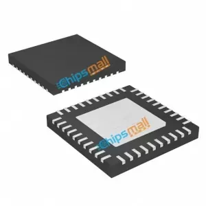

MAX1211ETL+T
- Manufacturer’s Part#:MAX1211ETL+T
- Manufacturer:
- Categories:
- Sub-Categories:
- Series:-
- ECAD Model:
- Description:IC ADC 12BIT 65MSPS 40-TQFN
- Datasheet:
- Quantity:RFQAdd to RFQ List
- Payment:

- Delivery:

- In Stock: 10740
- Price: please call
- Available: 10740
Required: Fill out the form, we will reply you ASAP.
- Description
- Alternatives
- Shopping Guide
The MAX1211 is a 3.3V, 12-bit analog-to-digital converter (ADC) featuring a fully differential wideband track-and-hold (T/H) input, driving the internal quantizer.
The MAX1211 is optimized for low power, small size, and high dynamic performance in intermediate frequency (IF) sampling applications. This ADC operates from a single 3.0V to 3.6V supply, consuming only 358mW while delivering a typical signal-to-noise ratio (SNR) performance of 66dB at an input frequency of 175MHz.
The T/H driven input stage accepts single-ended or differential inputs. In addition to low operating power, the MAX1211 features a 13mW power-down mode to conserve power during idle periods.A flexible reference structure allows the MAX1211 to use its internal precision bandgap reference or accept an externally applied reference.
The MAX1211 supports both a single-ended and differential input clock drive. Wide variations in the clock duty cycle are compensated with the ADC’s internal duty-cycle equalizer.
The MAX1211 features parallel, CMOS-compatible outputs.
The digital output format is pin selectable to be either two’s complement or Gray code. A separate power input for the digital outputs accepts a voltage from 1.7V to 3.6V for flexible interfacing with various logic levels.
The MAX1211 is available in a 6mm x 6mm x 0.8mm, 40-pin thin QFN package with exposed paddle (EP), and is specified for the extended industrial (-40°C to +85°C) temperature range.
Features
♦ Direct IF Sampling Up to 400MHz
♦ Excellent Dynamic Performance 66dB SNR at fIN = 175MHz 76dBc SFDR at fIN = 175MHz
♦ Differential or Single-Ended Clock
♦ 3.3V Low-Power Operation 358mW (Differential Clock Mode) 327mW (Single-Ended Clock Mode)
♦ Accepts 20% to 80% Clock Duty Cycle
♦ Fully Differential or Single-Ended Analog Input
♦ Wide ±1VP-P Differential Analog Input Voltage Range
♦ 700MHz Input Bandwidth
♦ Power-Down Mode
♦ CMOS-Compatible Outputs in Two’s Complement or Gray Code
♦ Out-of-Range and Data Valid Indicators
♦ Small, 40-Pin Thin QFN Package with Exposed Paddle
♦ Evaluation Kit Available (Order MAX1211EVKIT)Applications IF and Baseband Communication Receivers Cellular, LMDS, Point-to-Point Microwave, MMDS, HFC, WLAN Ultrasound and Medical Imaging Portable Instrumentation Low-Power Data Acquisition
Functional Equivalent (FE) materials, including Fused Filament Fabrication (FFF) form, assembly, and functionally compatible substitute materials.
SHIPPING GUIDE
Shipping Methods

Rest assured that your orders will be handled by these trusted providers, such as DHL, FedEx, SF, and UPS.
Shipping Cost

Shipping starts at $40 but varies for destinations like South Africa, Brazil, India, and more. The actual shipping charges depend on time zone, country, and package weight/volume.
Delivery Time

We ship orders once daily, around 5 p.m., except on Sundays. The estimated delivery time may vary depending on the courier service you choose, but typically ranges from 5 to 7 business days.

Professional Platform

Full-speed Delivery

Wide Variety of Products

365 Days of Quality Assurance


