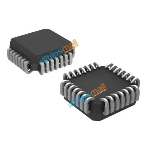

MC10E196FNG
- Manufacturer’s Part#:MC10E196FNG
- Manufacturer:
- Categories:
- Sub-Categories:
- Series:10E
- ECAD Model:
- Description:IC DELAY LINE 128TAP PROG 28PLCC
- Datasheet:
- Quantity:RFQAdd to RFQ List
- Payment:

- Delivery:

- In Stock: 10665
- Price: please call
- Available: 10665
Required: Fill out the form, we will reply you ASAP.
- Description
- Alternatives
- Shopping Guide
The MC10E/100E196 is a programmable delay chip (PDC) designed primarily for very accurate differential ECL input edge placement applications.
The delay section consists of a chain of gates and a linear ramp delay adjust organized as shown in the logic symbol.
The first two delay elements feature gates that have been modified to have delays 1.25 and 1.5 times the basic gate delay of approximately 80 ps.
These two elements provide the E196 with a digitally-selectable resolution of approximately 20 ps.
The required device delay is selected by the seven address inputs D[0:6], which are latched on chip by a high signal on the latch enable (LEN) control.
The FTUNE input takes an analog voltage and applies it to an internal linear ramp for reducing the 20 ps Least Significant Bit (LSB) minimum resolution still further.
The FTUNE input is what differentiates the E196 from the E195.An eighth latched input, D7, is provided for cascading multiple PDC’s for increased programmable range.
The cascade logic allows full control of multiple PDC’s, at the expense of only a single added line to the data bus for each additional PDC, without the need for any external gating.
The VBB pin, an internally generated voltage supply, is available to this device only. For single-ended input conditions, the unused differential input is connected to VBB as a switching reference voltage.VBB may also rebias AC coupled inputs. When used, decouple VBB and VCC via a 0.01 μF capacitor and limit current sourcing or sinking to 0.5 mA. When not used, VBB should be left open.
The 100 Series contains temperature compensation.
Features
• 2.0 ns Worst Case Delay Range
• ≈20 ps/Delay Step Resolution
• Linear Input for Tighter Resolution
• >1.0 GHz Bandwidth
• On Chip Cascade Circuitry
• PECL Mode Operating Range: VCC = 4.2 V to 5.7 V with VEE = 0 V
• NECL Mode Operating Range: VCC = 0 V with VEE = −4.2 V to −5.7 V
• Internal Input 50 kΩ Pulldown Resistors
• ESD Protection: Human Body Model; > 1 kV, Machine Model; > 75 V
• Meets or Exceeds JEDEC Spec EIA/JESD78 IC Latchup Test
• Moisture Sensitivity Level: Pb = 1; Pb−Free = 3 For Additional Information, see Application Note AND8003/D
• Flammability Rating: UL 94 V−0 @ 1.125 in, Oxygen Index: 28 to 34
• Transistor Count = 425 devices
• Pb−Free Packages are Available
*
Functional Equivalent (FE) materials, including Fused Filament Fabrication (FFF) form, assembly, and functionally compatible substitute materials.
SHIPPING GUIDE
Shipping Methods

Rest assured that your orders will be handled by these trusted providers, such as DHL, FedEx, SF, and UPS.
Shipping Cost

Shipping starts at $40 but varies for destinations like South Africa, Brazil, India, and more. The actual shipping charges depend on time zone, country, and package weight/volume.
Delivery Time

We ship orders once daily, around 5 p.m., except on Sundays. The estimated delivery time may vary depending on the courier service you choose, but typically ranges from 5 to 7 business days.

Professional Platform

Full-speed Delivery

Wide Variety of Products

365 Days of Quality Assurance


