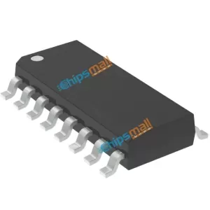

MC74VHCT139ADG
- Manufacturer’s Part#:MC74VHCT139ADG
- Manufacturer:
- Categories:
- Sub-Categories:
- Series:74VHCT
- ECAD Model:
- Description:IC DCODER/DMUX DUAL 2-4 16-SOIC
- Datasheet:
- Quantity:RFQAdd to RFQ List
- Payment:

- Delivery:

- In Stock: 604846
- Available: 15
Reference Price(In US Dollars)
| Qty | Unit Price | Ext.Price |
|---|---|---|
| 1+ | US $0.35886 | US $0.36 |
| 10+ | US $0.23924 | US $2.39 |
| 30+ | US $0.17943 | US $5.38 |
| 100+ | US $0.14354 | US $14.35 |
| 500+ | US $0.13158 | US $65.79 |
| 1000+ | US $0.11962 | US $119.62 |
Do you want a lower wholesale price? Please send us an inquiry, and we will respond immediately.
- Description
- Alternatives
- Shopping Guide
The MC74VHCT139A is an advanced high speed CMOS 2−to−4 decoder/demultiplexer fabricated with silicon gate CMOS technology. It achieves high speed operation similar to equivalent Bipolar Schottky TTL devices while maintaining CMOS low power dissipation.When the device is enabled (E = low), it can be used for gating or as a data input for demultiplexing operations. When the enable input is held high, all four outputs are fixed high, independent of other inputs.
The internal circuit is composed of three stages, including a buffer output which provides high noise immunity and stable output.
The device output is compatible with TTL−type input thresholds and the output has a full 5.0 V CMOS level output swing.
The input protection circuitry on this device allows overvoltage tolerance on the input, allowing the device to be used as a logic−level translator from 3.0 V CMOS logic to 5.0 V CMOS logic, or from 1.8 V CMOS logic to 3.0 V CMOS logic while operating at the high−voltage power supply
The MC74VHCT139A input structure provides protection when voltages up to 7.0 V are applied, regardless of the supply voltage. This allows the MC74VHCT139A to be used to interface 5.0 V circuits to 3.0 V circuits.
The output structures also provide protection when VCC = 0 V.
These input and output structures help prevent device destruction caused by supply voltage−input/output voltage mismatch, battery backup, hot insertion, etc.
Features
• High Speed: tPD = 5.0 ns (Typ) at VCC = 5.0 V
• Low Power Dissipation: ICC = 4 μΑ (Max) at TA = 25°C
• TTL−Compatible Inputs: VIL = 0.8 V; VIH = 2.0 V
• Power Down Protection Provided on Inputs and Outputs
• Balanced Propagation Delays
• Designed for 2.0 V to 5.5 V Operating Range
• Low Noise: VOLP = 0.8 V (Max)
• Pin and Function Compatible with Other Standard Logic Families
• Latchup Performance Exceeds 300 mA
• ESD Performance: Human Body Model > 2000 V; Machine Model > 200 V
• Chip Complexity: 100 FETs or 25 Equivalent Gates
•
These Devices are Pb−Free and are RoHS Compliant
Functional Equivalent (FE) materials, including Fused Filament Fabrication (FFF) form, assembly, and functionally compatible substitute materials.
SHIPPING GUIDE
Shipping Methods

Rest assured that your orders will be handled by these trusted providers, such as DHL, FedEx, SF, and UPS.
Shipping Cost

Shipping starts at $40 but varies for destinations like South Africa, Brazil, India, and more. The actual shipping charges depend on time zone, country, and package weight/volume.
Delivery Time

We ship orders once daily, around 5 p.m., except on Sundays. The estimated delivery time may vary depending on the courier service you choose, but typically ranges from 5 to 7 business days.

Professional Platform

Full-speed Delivery

Wide Variety of Products

365 Days of Quality Assurance


