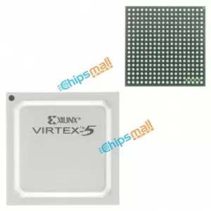

XC2C512-10FG324C
- Manufacturer’s Part#:XC2C512-10FG324C
- Manufacturer:
- Categories:
- Sub-Categories:
- Series:CoolRunner II
- ECAD Model:
- Description:IC CPLD 512MC 9.2NS 324BGA
- Datasheet:
- Quantity:RFQAdd to RFQ List
- Payment:

- Delivery:

- In Stock: 1154
- Available: 10
Reference Price(In US Dollars)
| Qty | Unit Price | Ext.Price |
|---|---|---|
| 1+ | US $116.55000 | US $116.55 |
| 10+ | US $90.65000 | US $906.50 |
| 30+ | US $77.70000 | US $2331.00 |
| 100+ | US $71.22500 | US $7122.50 |
| 500+ | US $68.63500 | US $34317.50 |
| 1000+ | US $64.75000 | US $64750.00 |
Do you want a lower wholesale price? Please send us an inquiry, and we will respond immediately.
- Description
- Alternatives
- Shopping Guide
The XC226x derivatives are high-performance members of the Infineon XC2000 Family of full featured single-chip CMOS microcontrollers.
These devices extend the functionality and performance of the C166 Family in terms of instructions (MAC unit), peripherals, and speed.
They combine high CPU performance (up to 66 million instructions per second) with high peripheral functionality and enhanced IO-capabilities. Optimized peripherals can be adapted to the application’s requirements in a flexible way.
These derivatives also provide clock generation via PLL and internal or external clock sources, and various on-chip memory modules such as program Flash, program RAM, and data RAM.Summary of
FeaturesFor a quick overview or reference, the XC226x’s properties are listed here in a condensed way.
• High Performance 16-bit CPU with 5-Stage Pipeline
– 15 ns Instruction Cycle Time at 66 MHz CPU Clock (Single-Cycle Execution)
– 1-Cycle 32-bit Addition and Subtraction with 40-bit result
– 1-Cycle Multiplication (16 × 16 bit)
– 1-Cycle Multiply-and-Accumulate (MAC) Instructions
– Background Division (32 / 16 bit) in 21 Cycles
– Enhanced Boolean Bit Manipulation Facilities
– Zero-Cycle Jump Execution
– Additional Instructions to Support HLL and Operating Systems
– Register-Based Design with Multiple Variable Register Banks
– Fast Context Switching Support with Two Additional Local Register Banks
– 16 Mbytes Total Linear Address Space for Code and Data
– 1024 Bytes On-Chip Special Function Register Area (C166 Family Compatible)
• 16-Priority-Level Interrupt System with up to 87 Sources, Selectable External Inputs for Interrupt Generation and Wake-Up, Sample-Rate down to 15 ns
• 8-Channel Interrupt-Driven Single-Cycle Data Transfer Facilities via Peripheral Event Controller (PEC), 24-Bit Pointers Cover Total Address Space
• Clock Generation from Internal or External Clock Sources, via on-chip PLL or via Prescaler
• On-Chip Memory Modules
– 1 Kbyte On-Chip Stand-By RAM (SBRAM)
– 2 Kbytes On-Chip Dual-Port RAM (DPRAM)
– 16 Kbytes On-Chip Data SRAM (DSRAM)
– Up to 64 Kbytes On-Chip Program/Data SRAM (PSRAM)
– Up to 768 Kbytes On-Chip Program Memory (Flash Memory)
• On-Chip Peripheral Modules
– Two Synchronizable A/D Converters with a total of 16 Channels, 10-bit Resolution, Conversion Time down to 1.2 µs, Optional Data Preprocessing (Data Reduction, Range Check)
– 16-Channel General Purpose Capture/Compare Unit (CAPCOM2)
– Up to four Capture/Compare Units for flexible PWM Signal Generation (CCU6x)
– Multi-Functional General Purpose Timer Unit with 5 Timers
– Six Serial Interface Channels to be used as UART, LIN, High-Speed Synchronous Channel (SPI/QSPI), IIC Bus Interface (10-bit addressing, 400 kbit/s), IIS Interface
– On-Chip MultiCAN Interface (Rev. 2.0B active) with up to 128 Message Objects (Full CAN/Basic CAN) on up to 5 CAN Nodes and Gateway Functionality
– On-Chip Real Time Clock
• Up to 12 Mbytes External Address Space for Code and Data
– Programmable External Bus Characteristics for Different Address Ranges
– Multiplexed or Demultiplexed External Address/Data Buses
– Selectable Address Bus Width
– 16-Bit or 8-Bit Data Bus Width
– Four Programmable Chip-Select Signals
• Single Power Supply from 3.0 V to 5.5 V
• Power Reduction Modes with Flexible Power Management
• Programmable Watchdog Timer and Oscillator Watchdog
• Up to 75 General Purpose I/O Lines
• On-Chip Bootstrap Loader
• Supported by a Large Range of Development Tools like C-Compilers, Macro-Assembler Packages, Emulators, Evaluation Boards, HLL-Debuggers, Simulators, Logic Analyzer Disassemblers, Programming Boards
• On-Chip Debug Support via JTAG Interface
• 100-Pin Green LQFP Package, 0.5 mm (19.7 mil) pitch
Functional Equivalent (FE) materials, including Fused Filament Fabrication (FFF) form, assembly, and functionally compatible substitute materials.
SHIPPING GUIDE
Shipping Methods

Rest assured that your orders will be handled by these trusted providers, such as DHL, FedEx, SF, and UPS.
Shipping Cost

Shipping starts at $40 but varies for destinations like South Africa, Brazil, India, and more. The actual shipping charges depend on time zone, country, and package weight/volume.
Delivery Time

We ship orders once daily, around 5 p.m., except on Sundays. The estimated delivery time may vary depending on the courier service you choose, but typically ranges from 5 to 7 business days.

Professional Platform

Full-speed Delivery

Wide Variety of Products

365 Days of Quality Assurance


