


OUTLINE:
Field Effect Transistors (FETs): Types, Operation, and Applications
 288
288A transistor is a tiny device that controls the flow of electricity in a circuit. It works like a switch or a gate. You can use it to turn a signal on or off, or even to amplify a weak signal.
One special type of transistor is the Field Effect Transistor, or FET for short. It doesn't require a current to work, unlike some other transistors. Instead, it uses voltage to control the flow of current. That’s why people say it’s voltage-controlled.
FETs are very common in modern electronics. You can find them in phones, laptops, radios, and various digital devices. Let’s learn how FETs work, the different types available, and where they are used in everyday tech.

What is a Field Effect Transistor (FET)
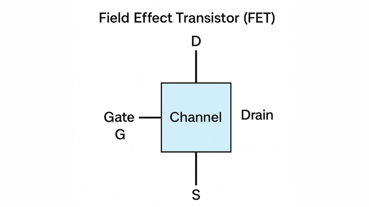
A Field Effect Transistor (FET) is a type of transistor used to manage electrical signals in a circuit. It controls the flow of current between two terminals—called the source and the drain—by using a third terminal known as the gate.
Instead of relying on current, the gate uses voltage to regulate this flow, making the device efficient and easy to control. Because of this feature, FETs are widely used in everything from amplifiers to digital processors.
Historical Development and Evolution
The story of the Field Effect Transistor (FET) began in 1925, when Austrian physicist Julius Edgar Lilienfeld first proposed the idea of a device that could control electrical current using an electric field. However, due to limitations in materials and technology at the time, his concept could not be built successfully.
In the 1950s, the first practical form of the FET, the Junction Field Effect Transistor (JFET), was developed. It was a significant milestone in transistor technology and provided a new approach to signal amplification using a voltage-controlled method.
The breakthrough came in 1959 when Mohamed Atalla and Dawon Kahng at Bell Labs invented the Metal-Oxide-Semiconductor Field Effect Transistor (MOSFET). Its structure included an insulated gate made with silicon dioxide, which allowed for better control, miniaturization, and scalability.
During the 1970s, the MOSFET began to dominate the semiconductor industry. It became the backbone of digital electronics and integrated circuits (ICs) due to its low power consumption and ease of integration.
Over time, MOSFET technology evolved from planar structures to more advanced forms such as FinFETs and Gate-All-Around (GAA) transistors, enabling even smaller, faster, and more efficient chips used in modern microprocessors and memory devices.
Structure and Basic Operation of a FET
Terminals of a FET: A Field Effect Transistor (FET) includes three main terminals:
-
Gate (G): This terminal receives the voltage signal. It creates an electric field that controls the current flow through the transistor.
-
Source (S): This is the terminal where current enters the transistor.
-
Drain (D): This is where the current exits the transistor.
-
Body or Substrate: Some FETs also have a fourth terminal called the Body or Substrate. This part connects to the underlying semiconductor material. In most circuits, the body is connected to the source terminal to prevent unwanted current paths.
How does it work?
The FET works by using an electric field to control the flow of current. Inside the device, there is a path called the channel between the source and drain. This channel is made of semiconductor material.
FETs come in two types based on the kind of semiconductor in the channel:
-
N-channel FET: The channel is made of N-type material. A positive voltage at the gate allows current to flow.
-
P-channel FET: The channel is made of P-type material. A negative voltage at the gate allows current to flow.
Two modes define the behavior of the FET:
-
Depletion mode: The channel is conducted by default. Gate voltage reduces the current flow.
-
Enhancement mode: The channel does not conduct unless a voltage is applied at the gate.
Types of Field Effect Transistors
-
Junction Field Effect Transistor (JFET): The JFET uses a p-n junction as its gate. It has either N-channel or P-channel designs. In JFETs, the current always flows through the channel unless the gate voltage reduces it. So, all JFETs operate in depletion mode.
No gate current flows, but applying reverse voltage at the gate changes the width of the channel, controlling the flow. This control makes JFETs good for analog signal amplification, like in microphones, radios, and sensors.
-
Metal-Oxide-Semiconductor Field Effect Transistor (MOSFET): The MOSFET is the most used type of FET. It features an insulated gate made using a metal-oxide layer (usually silicon dioxide). Because of the gate insulation, the MOSFET draws almost no gate current, which makes it very efficient.
MOSFETs have two subtypes:
-
Enhancement-mode MOSFET
-
The channel is normally OFF.
-
A voltage at the gate creates a channel and allows current to flow.
-
Common in digital circuits like computers and memory.
-
-
Depletion-mode MOSFET
-
The channel is normally ON.
-
Applying a gate voltage reduces or stops current flow.
-
CMOS (Complementary MOS) technology combines n-MOS and p-MOS MOSFETs. It helps build logic gates that use less power, making CMOS the standard for modern digital ICs, including processors and memory chips.
MOSFETs support very small sizes. Thousands or millions of them fit on a tiny chip using VLSI (Very-Large-Scale Integration) and ULSI (Ultra-Large-Scale Integration) technology. This feature makes MOSFETs the heart of today’s electronics.
3. Metal-Semiconductor FET (MESFET): The MESFET uses a metal-semiconductor (Schottky) junction instead of a p-n junction. This design gives it faster switching and better performance at high frequencies.
MESFETs are built using materials like gallium arsenide (GaAs) or indium phosphide (InP). These materials allow faster electron movement than silicon. MESFETs are used in RF (radio frequency) and microwave applications, like satellite receivers and wireless communication systems.
4. Other FET Variants
-
IGBT (Insulated-Gate Bipolar Transistor): This device combines a MOSFET input with a BJT output. It handles high power and high voltage, which makes it useful in motor drives, electric vehicles, and industrial machines.
-
OFET (Organic Field Effect Transistor): Made with organic materials. These FETs are flexible and printable, which makes them ideal for wearable tech, bendable displays, and biosensors.
-
CNTFET (Carbon Nanotube FET): Uses carbon nanotubes instead of silicon. It operates at very small scales. Still under development, this FET shows potential in future nanoelectronics and energy-efficient processors.
-
FinFET (Fin Field Effect Transistor): Uses a 3D fin-like structure for the channel. This shape gives better control over current and reduces leakage. FinFETs are used in modern processors (like Intel and AMD chips) and allow more transistors on one chip for faster and smaller devices.
Key Characteristics and Performance Metrics
-
Input Impedance: FETs have very high input resistance, which means they don’t load the circuit they’re connected to. This makes them excellent for signal amplification.
-
Transconductance (gm): This measures how well the gate voltage controls the current between the source and drain. A higher transconductance means better control and stronger amplification.
-
Threshold Voltage (Vth): This is the minimum voltage needed at the gate to allow current to start flowing from the source to the drain.
-
Saturation Region and Linear Region: The FET operates in different regions based on gate and drain voltages. In the saturation region, the current stays steady and is ideal for amplifiers. In the linear region, current changes with voltage and suits switching applications.
-
On-Resistance (Rds(on)): This is the resistance between the source and drain when the FET is turned ON. Lower resistance leads to higher efficiency in switching.
-
Breakdown Voltage: This is the maximum voltage the FET can handle before the device gets damaged. FETs must be chosen based on the voltage levels in the circuit.
-
Gate Capacitance: The gate has a small capacitance due to the insulation layer. This affects how fast the FET can switch. Lower capacitance allows higher switching speed.
Advantages of FETs Over BJTs
1. Higher Input Impedance
FETs have extremely high input impedance, often several megaohms or more. This means they draw almost no current from the input source. As a result, FETs do not load down or affect the behavior of preceding circuit stages. This characteristic makes them ideal for use in buffer and amplification circuits where maintaining signal integrity is critical.
2. Lower Power Consumption
Since FETs are controlled by voltage rather than current, they consume significantly less power than BJTs. The gate of a FET acts like a capacitor, requiring only a small charge to operate. This minimal power requirement makes FETs well-suited for energy-efficient devices such as smartphones, laptops, and other portable electronics.
3. Better Thermal Stability
FETs offer greater thermal stability than BJTs. In BJTs, increased temperature causes an increase in current, which can lead to thermal runaway. FETs, on the other hand, tend to self-regulate—their current either remains stable or slightly decreases with rising temperature. This property helps maintain reliable operation across a range of environmental conditions.
4. Smaller Size and Easier Integration
FETs, especially MOSFETs, can be manufactured at very small sizes. This allows them to be densely packed onto a single silicon chip. Their compact size supports large-scale integration in modern microelectronics, including VLSI (Very-Large-Scale Integration) and ULSI (Ultra-Large-Scale Integration) technologies, enabling the production of powerful yet compact processors and memory units.
5. Faster Switching Speeds
FETs switch on and off more quickly than BJTs because they do not rely on charge carrier injection. Their fast switching ability makes them highly effective in digital logic circuits and high-frequency applications such as microprocessors, RF transmitters, and switching power supplies. This speed also contributes to reduced power loss and higher circuit efficiency.
Common Applications of FETs
-
Amplification: FETs are widely used in amplifier circuits due to their high input impedance and low noise characteristics. In audio amplification, they help preserve sound quality by avoiding signal loss from input loading. In radio-frequency (RF) amplifiers, their fast switching speed and low parasitic capacitance make them ideal for handling high-frequency signals. Their ability to work with minimal noise interference also makes them suitable for low-noise amplifiers in sensitive applications like medical equipment and precision instrumentation.
-
Switching: FETs, especially MOSFETs, dominate in switching applications due to their fast response and low power loss. In logic gates and digital integrated circuits (ICs), MOSFETs act as the basic switching elements that turn on and off rapidly to process binary data. In power electronics, they are used in switch-mode power supplies (SMPS) and motor control systems, providing efficient power regulation and load handling. FETs are also found in load switches for both low-voltage portable devices and high-voltage industrial systems.
-
Analog and Mixed Signal Applications: FETs are used in a range of analog and hybrid analog-digital circuits. As buffers, they isolate different circuit stages without affecting the signal. In oscillators, FETs help generate repeating signals for use in clocks and transmitters. They also function in analog switches, sample-and-hold circuits, and voltage-controlled resistors, where signal precision and minimal distortion are critical.
-
Specialized Applications: In cutting-edge fields, special types of FETs are being applied in innovative ways. Organic FETs (OFETs) are used in biosensors for detecting chemical or biological signals. FinFETs, with their 3D structure, are now a standard in modern microprocessors due to their superior control and reduced leakage. FETs also serve in memory technologies like DRAM and SRAM, storing data efficiently. Additionally, their flexibility and low power make them ideal for wearable electronics and flexible display systems.
Handling, Protection & ESD Sensitivity
FETs, especially MOSFETs, are highly sensitive to electrostatic discharge (ESD) due to their insulated gate structure. To prevent damage, it is essential to follow proper ESD protection protocols during handling and assembly.
Technicians should always wear antistatic wrist straps that are correctly grounded to prevent static buildup and discharge. Components should be stored in antistatic bags, foam, or conductive tubes when not in use, keeping them safe from electrostatic environments.
During soldering and PCB assembly, work should be done on ESD-safe mats using ESD-protected tools and equipment. Even when moving FETs around the lab or production floor, they should remain in their protective packaging until installation.
Following these precautions helps avoid permanent damage to the device and ensures long-term reliability and performance in the final application.

Modern Trends and Future of FET Technology
-
Nano-scale MOSFETs and Moore’s Law: The push for smaller, faster, and more efficient electronics continues to drive the miniaturization of FETs. Nano-scale MOSFETs are now standard in advanced microchips, keeping up with Moore’s Law, which projected that the number of transistors on a chip would double approximately every two years. However, as silicon approaches its physical limits, new solutions are required.
-
FinFETs and Gate-All-Around (GAA) FETs: To tackle short-channel effects and leakage problems at small sizes, manufacturers have moved from traditional planar designs to 3D transistor architectures like FinFETs. These offer improved control over current flow. Gate-All-Around (GAA) FETs, a further advancement, allow the gate to fully surround the channel, giving even better electrostatic control and efficiency.
-
Emerging Materials: Graphene and CNTs: Researchers are exploring alternative materials to replace silicon. Graphene and carbon nanotubes (CNTs) promise higher conductivity, faster switching, and reduced power usage. These materials are being studied for future ultra-fast, low-power transistors that could redefine electronics.
-
Flexible Electronics and Organic Semiconductors: Organic FETs (OFETs) made from plastic-like semiconductors are enabling flexible, stretchable, and even wearable electronics. These are ideal for medical patches, foldable devices, and soft robotics applications where rigid silicon is unsuitable.
-
Energy-Efficient and AI-Capable Transistors: Modern computing needs are driving the development of energy-efficient transistors for AI processing, edge computing, and mobile devices. These transistors must operate at high speeds while consuming minimal power, which is now a key design focus in FET engineering.
-
Role in Quantum and Neuromorphic Computing: FETs may also contribute to quantum computing and neuromorphic circuits (systems that mimic the brain’s structure). Specialized FET designs are being tested as quantum control elements or artificial synapses in advanced, futuristic processors.
If you're looking for a reliable source to purchase FETs, Chipsmall is highly recommended. With a strong reputation for distributing authentic and hard-to-find semiconductor components, Chipsmall offers excellent service and global delivery, making it a trusted partner for professionals and hobbyists alike.
Chipsmall:
Chipsmall is headquartered in Hong Kong. It is a professional distributor of electronic components, specializing in original and hard-to-find semiconductors, including FETs, MOSFETs, and other essential chips. The company has over 20 years of industry experience and has built a strong global reputation for authenticity, fast delivery, and competitive pricing.
Chipsmall serves clients across Europe, America, and South Asia, offering a vast inventory of components from leading brands. For engineers, manufacturers, and purchasing teams, Chipsmall is a highly recommended source for all your electronic components needs.
FAQs
Q1. Why is the gate of an FET not supposed to draw any current?
A: Because FETs are voltage-controlled devices, the gate is electrically insulated from the channel (especially in MOSFETs). This means almost no current flows into the gate, allowing for extremely high input impedance and minimal loading of the previous circuit stage.
Q2. Can FETs be used in both analog and digital applications?
A: Yes. FETs are extremely versatile—used in analog applications like audio amplifiers and oscillators, as well as in digital circuits such as logic gates, microprocessors, and memory cells.
Q3. What happens if I apply too much voltage to the gate of an FET?
A: Applying excessive voltage to the gate—especially without proper protection—can break down the thin insulating layer, permanently damaging the device. This is why voltage ratings and ESD precautions are crucial.
Q4. Why are FETs preferred over BJTs in modern electronics?
A: FETs offer lower power consumption, faster switching, and are easier to scale down, making them ideal for integrated circuits (ICs). Their high input impedance also makes them great for signal amplification with minimal distortion.
Q5. Are all FETs the same in terms of performance?
A: Not at all. Different types—JFETs, MOSFETs, MESFETs, FinFETs, etc.—offer unique characteristics like speed, voltage control, frequency range, and power handling. Choosing the right FET depends on the application.
Q6. Why do some FETs have a fourth terminal?
A: Some FETs include a body (or substrate) terminal, which can affect performance depending on the voltage between the body and source. In ICs, this is often internally connected, but in discrete FETs, it's sometimes accessible for biasing or grounding.
Conclusion
FETs are important in electronics because they control current using voltage. That makes them different from other transistors—and super useful.
They work great in both digital circuits (like computers and smartphones) and analog devices (like amplifiers and radios). From simple audio setups to advanced microprocessors, FETs fit just about everywhere.
The best part is they keep getting better. New materials like graphene and carbon nanotubes, plus new shapes like FinFETs, are pushing FETs into the future.
Whether it’s powering your phone or running AI chips, FETs are here to stay, and they’re only going to get smarter and more powerful
Disclaimer: The views and opinions expressed by individual authors or forum participants on this website do not represent the views and opinions of Chipsmall, nor do they represent Chipsmall's official policy.

share this blog to: